
(5.1) Introduction
Chapter 4 introduced the basic building blocks of a computer: transistors, gates, and circuits. This chapter puts those blocks together to build the major sub-systems of a computer.
(5.2) The Components of a Computer System
The earliest computing devices were programmed by punching up a deck of IBM cards and/or wiring up a plug-board. In 1946, John von Neumann suggested it would be better to store the program for a computing device in the same memory as its data so it could fetch its instructions at a fast rate and also operate on its own program if need be. We call this the stored program concept.
Figure 5.2 shows the major sub-systems of a computer with the Von Neumann Architecture. The architecture has a Memory holding both data and instructions to be executed by a computer; a Processor comprising an Arithmetic-Logic Unit (ALU) to operate on the data under control of a Control Unit executing instructions read from memory one at a time; and Input-Output devices to input data and programs from the outside world and to send results to the outside world.
(5.2.1) Memory and Cache: The state of each memory bit is held in a bi-stable device called a flip-flop. There are many different ways to implement a flip-flop from the basic logic gates - the following diagram shows a flip-flop built from a NOT-gate, an AND-gate, and an OR-gate:
Raising the S input of this flip-flop to the 1-value sets the state of its stored bit, Q, to the 1-state. Raising the R input to the 1-value resets the state of Q to the 0-state. When S = R = 0 the flip-flop acts like a memory and holds the current state of its stored bit, Q. The computer should never try to both set and reset the flip-flop at the same time; i.e., it should never raise both inputs S and R to the 1-value simultaneously.
There are only two inputs, S and R, in this circuit but to see how the flip-flop behaves we must also consider the current state of the stored bit, Q, and draw a truth table with 8 rows:
| INPUTS | Current state of Q |
Internal Lines | New state of Q = S OR b | ||
|---|---|---|---|---|---|
| S | R | a = NOT(R) | b = a AND Q | ||
| 0 | 0 | 0 | 1 | 0 | 0 |
| 0 | 0 | 1 | 1 | 1 | 1 |
| 0 | 1 | 0 | 0 | 0 | 0 |
| 0 | 1 | 1 | 0 | 0 | 0 |
| 1 | 0 | 0 | 1 | 0 | 1 |
| 1 | 0 | 1 | 1 | 1 | 1 |
| 1 | 1 | 0 | Not Allowed | ||
| 1 | 1 | 1 | |||
From the truth table we see that the flip-flop behaves like it should:
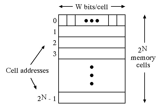
| N | Address Space (in bytes) | Usually Written |
|---|---|---|
| 16 | 65,536 | 64 Kilobytes |
| 20 | 1,048,576 | 1 Megabyte |
| 22 | 4,194,304 | 4 Megabytes |
| 24 | 16,777,216 | 16 Megabytes |
| 26 | 67,108,864 | 64 Megabytes |
| 28 | 268,435,456 | 256 Megabytes |
| 30 | 1,073,741,824 | 1 Gigabyte |
| 32 | 4,294,967,296 | 4 Gigabytes |
| 40 | 1,099,511,627,776 | 1 Terabyte |
The metric system of measurements uses certain prefixes for certain powers of ten:
| kilo | 103 = 1,000 |
|---|---|
| mega | 106 = 1,000,000 |
| giga | 109 = 1,000,000,000 |
| tera | 1012 = 1,000,000,000,000 |
| peta | 1015 = 1,000,000,000,000,000 |
The computer field only does this with memory capacities - all other quantities are measured with powers of ten. For example, an 800-megahertz clock emits exactly 800,000,000 clock ticks per second and a network link with a 10-megabyte/second bandwidth transmits exactly 10,000,000 bytes per second across the link.
A text string of m characters occupies m successive bytes of a RAM with each byte holding the ASCII code for one character. For example, the 10-character string, KENT STATE, might occupy bytes 160 through 169 of a RAM as follows:
| ADDRESS | CONTENTS | ASCII-Character |
|---|---|---|
| 160 | 01001011 | K |
| 161 | 01000101 | E |
| 162 | 01001110 | N |
| 163 | 01010100 | T |
| 164 | 00100000 | (space) |
| 165 | 01010011 | S |
| 166 | 01010100 | T |
| 167 | 01000001 | A |
| 168 | 01010100 | T |
| 169 | 01000101 | E |
The Memory Unit also has a Memory Address Register (MAR) and a Memory Data Register (MDR) for communication with other parts of the computer. The MAR holds the N-bit address of a memory cell and the MDR holds the data being fetched from that cell or the data being stored into that cell. The size of the MDR is some multiple of W bits and usually agrees with the size of the processor: e.g., a 32-bit processor can fetch or store 32 memory bits at one time so the MDR holds 4 bytes.
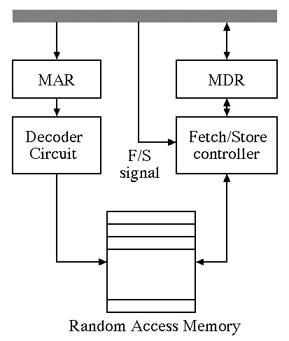
A memory fetch operation retrieves data from a storage location of the RAM using the following algorithm:
A large RAM is usually too slow for the processor so modern computers use a small fast cache memory as well as the RAM. Most computer programs exhibit a property called locality of reference: if the program has recently referenced a particular storage location in the RAM it will most likely want to reference the same location (or its neighbors) in the near future. The cache memory holds recently-referenced memory items and their neighbors so future references to these items can be performed much faster.
A Read-Only Memory (ROM) is a RAM without the store operation: its contents are fixed when it is built. One common use of a ROM is to initialize a computer properly whenever it is turned on.
(5.2.2) Input/Output and Mass Storage: There is a wide variety of input/output (I/O) devices that computers connect to:
Tapes are sequential access storage devices (SASDs). To find a particular data record on the tape the computer starts at the beginning of the tape and examines the records one at a time until it finds the one sought.
I/O devices are much slower than the other subsystems of a computer so the I/O controllers contain buffers to temporarily hold I/O data. The processor executes instructions while I/O data is being transferred.
(5.2.3) The Arithmetic/Logic Unit: The arithmetic/logic unit (ALU) is usually shown as a vee-shaped block to emphasize the fact that it combines two input numbers, A and B, with an arithmetic operation (add, subtract, multiply, etc.) to produce one number as a result. The operation is specified by a set of control lines fed by the Control Unit:

The ALU can also compare the two input numbers to see if A is Greater-Than, EQual to, or Less-Than B - for this operation the ALU sets one of the three condition-code bits (GT, EQ, or LT) to the 1-state.
To speed up arithmetic, modern computers couple the ALU with a set of very fast memory cells called registers. Figure 5.11 shows such a datapath with an ALU coupled to 16 registers, R0, R1, ..., R15. The organization is very flexible; for example, the ALU can subtract the value in any register from the value in any register and store the difference into any register. Storing the result of an ALU operation into a register overwrites the previous value stored in that register.
In a b-bit processor each register holds b bits and the ALU performs operations on b-bit data items (b is usually 32 or 64.)
(5.2.4) The Control Unit: The stored program concept means that machine instructions are stored in memory as sequences of binary bits. The control unit:
Each instruction is written in machine language as a sequence of 0-bits and 1-bits with a format like:
| Operation code | Address field 1 | Address field 2 | Address field 3 | . . . |
|---|
Each operation in the instruction set of the computer is assigned a unique unsigned-integer operation code (or opcode). For example, opcode 0 might specify the ADD operation, opcode 1 might specify the COMPARE operation, etc. An opcode field of k bits can specify any one of 2k different operations.
The address fields specify the locations of the source operands and the result of the operation. For example, an instruction to subtract the contents of register R2 from the contents of register R1 and put the difference in register R3 might look like:
| 0101 | 0001 | 0010 | 0011 |
|---|---|---|---|
| SUB | R1 | R2 | R3 |
where 0101 is the opcode for subtraction and each 4-bit address field specifies one of the sixteen registers. Address fields specifying memory locations are much longer since it takes an n-bit address to specify one of the locations in a 2n-byte RAM. Some processors use only two address fields for arithmetic operations - the result of an operation overwrites one of the source operands.
In the seventies and the eighties the typical processor had several hundred opcodes. The add operation, for example, might have three different opcodes:
These processors had variable-length instructions. For example, the ADD3 instruction required many more bytes than the ADDR instruction.
Machine languages for modern processors are much simpler with less than 50 operations. These machines are called Reduced Instruction Set Computers or RISC machines. Fixed-length instructions (usually 32 bits) are used and arithmetic operations only use register operands. Even though a RISC machine must execute more instructions to perform a typical algorithm, each instruction runs much faster so the running time of the algorithm is less.
There are four basic classes of instructions:
(5.3) Putting All the Pieces Together: Figure 5.18 shows the organization of a Von Neumann computer with a number of ALU registers: R0, R1, R2, R3, ...
Figure 5.19 shows a hypothetical instruction set for a Von Neumann computer:
| Binary Opcode | Operation | Meaning |
|---|---|---|
| 0000 | LOAD X | CON(X) --> R |
| 0001 | STORE X | R --> CON(X) |
| 0010 | CLEAR X | 0 --> CON(X) |
| 0011 | ADD X | R + CON(X) --> R |
| 0100 | INCREMENT X | CON(X) + 1 --> CON(X) |
| 0101 | SUBTRACT X | R - CON(X) --> R |
| 0110 | DECREMENT X | CON(X) - 1 --> CON(X) |
| 0111 | COMPARE X | if CON(X) > R then set GT to 1, else 0 if CON(X) = R then set EQ to 1, else 0 if CON(X) < R then set LT to 1, else 0 |
| 1000 | JUMP X | Jump to location X |
| 1001 | JUMPGT X | Jump to location X if GT = 1 |
| 1010 | JUMPEQ X | Jump to location X if EQ = 1 |
| 1011 | JUMPLT X | Jump to location X if LT = 1 |
| 1100 | JUMPNEQ X | Jump to location X if EQ = 0 |
| 1101 | IN X | Input an integer into location X |
| 1110 | OUT X | Output an integer from location X |
| 1111 | HALT | Stop program execution |
The control unit uses the following algorithm to execute a program.
| Set the PC to the address of the first instruction in the program. | |
| Repeat | until a HALT instruction or a fatal error is encountered. |
| Fetch phase | |
| Decode phase | |
| Execute phase | |
| End of the loop | |
Execute Phase: The steps in the execute phase depend on the opcode of the instruction. The steps for some of the instructions in figure 5.19 are shown below:
Figure 5.20 graphs processor speeds from the mid-1940s to the present. At first processor speeds grew exponentially - quadrupling about every three years. But lately the growth rate has been slower. To get higher processing speed several processing elements are coupled together in a parallel processor. Parallel processors come in two different flavors: SIMD and MIMD.
SIMD: Figure 5.21 is a block diagram of a Single-Instruction-Multiple-Data (SIMD) processor - several ALUs (usually in the thousands) reading and writing data in their own local memories under command of a single control unit executing instructions from a single program. For example, an ADD instruction in the program will cause every ALU to perform an ADD operation on its own data. Unfortunately, the figure doesn't show the interconnection network between the ALUs that every SIMD processor has.
MIMD: Figure 5.22 is a block diagram of a Multiple-Instruction-Multiple-Data (MIMD) processor - several processors (each with its own ALU and control unit) execute instructions from their own programs in their own local memories. For example, while some processors are executing ADD instructions others might be executing SUB instructions.
SIMD vs. MIMD: The single control unit in a SIMD processor keeps all ALUs in lock-step. This simplifies communication of data between the ALUs - a Data Transfer instruction in the program:
Inter-processor communication in a MIMD processor is much slower. For example, to send a data item from processor A to processor B, the program in A must be synchronized with the program in B so B expects to receive the item when A sends it.