Chapter 4 - The Building Blocks
(4.2) The Binary Numbering System
(4.2.1) Binary Representation of Numeric and TextualInformation:
Humans (at least those who speak English) use the following conventions
for representing information:
- Decimal digits for numerical values: 0, 1, 2, 3, 4, 5, 6, 7, 8, 9
- The 26 letters in the alphabet for textual information (plus
lower-case letters and special symbols for punctuation)
- Sign/magnitude notation for positive and negative numbers: e.g.,
-31 and +789
- Decimal notation for real numbers with a decimal point separating
the whole-number part from the fraction: e.g., 3.1416
These conventions are used when one enters information into a computer
through a keyboard and when the computer displays information on a printer
or screen but the computer uses different conventions when it stores and
processes information internally:
- Whole numbers are stored using a base-2 positional numbering
system where each binary digit (bit) has just two values: 0 or 1.
For example, the decimal number 57 is stored as the 6-digit binary number,
111001, because:
57 = 32 + 16 + 8 + 1 = 25 + 24 + 23
+ 20
and the weights of the six bits of the binary number are powers of two:
| Weight of bit |
25 | 24 | 23 |
22 | 21 | 20 |
|---|
| Bits of 6-bit number |
1 | 1 | 1 | 0 | 0 | 1 |
|---|
An n-bit binary number can store any whole number from 0 to
2n - 1: e.g., the range of a 16-bit number is from 0 to
216-1 = 65,535 and the range of a 32-bit number is from 0 to
232-1 = 4,294,967,295.
Problem: What decimal number is represented by the 32-bit binary number:
0000 0011 1111 1111 1111 1111 1111 0000
and did you find an easy way to calculate it?
- Negative whole numbers are stored using two's complement notation -
the bits of a number are weighted with powers of two except that the leftmost
bit is weighted with the negative of a power of two. For example, the 6-bit
sequence 111001 as a two's complement number has the value -7 because:
| Weight of bit |
-25 | 24 | 23 |
22 | 21 | 20 |
|---|
| Bits of 6-bit number |
1 | 1 | 1 | 0 | 0 | 1 |
|---|
and -7 = -32 + 16 + 8 + 1.
- Each real number is stored in scientific notation with a signed
fraction and a base-2 exponent.
- Textual information is stored using the American Standard Code for
Information Interchange (ASCII) which represents each character as an 8-bit
binary number:
ASCII Conversion Table
| Leftmost 5 bits |
Rightmost 3 bits |
|---|
| 000 | 001 | 010 | 011 |
100 | 101 | 110 | 111 |
|---|
| 00100 | (space) | ! | " | # |
$ | % | & | ' |
|---|
| 00101 | ( | ) | * | + |
, | - | . | / |
|---|
| 00110 | 0 | 1 | 2 | 3 |
4 | 5 | 6 | 7 |
|---|
| 00111 | 8 | 9 | : | ; |
< | = | > | ? |
|---|
| 01000 | @ | A | B | C |
D | E | F | G |
|---|
| 01001 | H | I | J | K |
L | M | N | O |
|---|
| 01010 | P | Q | R | S |
T | U | V | W |
|---|
| 01011 | X | Y | Z | [ |
\ | ] | ^ | _ |
|---|
| 01100 | ` | a | b | c |
d | e | f | g |
|---|
| 01101 | h | i | j | k |
l | m | n | o |
|---|
| 01110 | p | q | r | s |
t | u | v | w |
|---|
| 01111 | x | y | z | { |
| | } | ~ | |
|---|
Inside a computer every item of information, whether numerical or textual or
anything else, is stored as a sequence of 0's and 1's. How does a computer
know what a given sequence of 0's and 1's mean? Only by context. For example, if
the 8-bit sequence 01000001 is sent to a display screen then the screen
displays the ASCII-character, A, but if the same sequence is sent to an
adder that adds whole numbers then it is interpreted as the whole number 65.
(4.2.3) The Reliability of Binary Representation: Why do computers
represent information in binary form instead of decimal form?
Reliable bi-stable (2-state) devices are easy to build: it's very hard to
build a reliable storage device with ten states.
Some of the earliest computers performed their arithmetic on decimal numbers
but each decimal digit was stored in four or more bi-stable devices. Three
popular codes for representing decimal digits are shown in the following table:
Decimal
Digit | Binary Code
(4 bits) |
Excess-3
Code (4 bits)
| Bi-Quinary
Code (7 bits) |
|---|
| 0 | 0000 | 0011 | 10 10000 |
|---|
| 1 | 0001 | 0100 | 10 01000 |
|---|
| 2 | 0010 | 0101 | 10 00100 |
|---|
| 3 | 0011 | 0110 | 10 00010 |
|---|
| 4 | 0100 | 0111 | 10 00001 |
|---|
| 5 | 0101 | 1000 | 01 10000 |
|---|
| 6 | 0110 | 1001 | 01 01000 |
|---|
| 7 | 0111 | 1010 | 01 00100 |
|---|
| 8 | 1000 | 1011 | 01 00010 |
|---|
| 9 | 1001 | 1100 | 01 00001 |
|---|
Whatever the code, a decimal computer wastes storage capability: using only
10 of the 16 states of four bi-stable devices (or only 10 of the 128 states
of seven devices.) Modern computers use binary numbers because: all
the states of bi-stable devices can be used; binary arithmetic is easier than
decimal arithmetic; and it's easy to program a computer to convert between
binary and decimal on input and output.
(4.2.4) Binary Storage Devices: Binary computers use bi-stable devices.
A bi-stable device:
- has two stable energy states (a state for a 0 and a state for a 1);
- where the two states are separated by a large energy barrier (so that a 0
doesn't accidentally become a 1, or vice versa);
- where it is possible to sense what state the device is in (to see whether
it is storing a 0 or a 1) without permanently destroying the stored value; and
- where it is possible to switch the state from a 0 to a 1, or vice versa,
by applying a sufficient amount of energy.
Examples of bi-stable devices are: an ON-OFF light switch, a magnetic core, and
a transistor.
(4.3) Boolean Logic and Gates
(4.3.1) Boolean Logic: George Boole applied the formal laws
of algebra and arithmetic to the principles of logic. Each statement in logic
is either true or false and one can use the AND, OR, and NOT
operators to construct statements from other statements.
For example, consider the following three statements:
| A: | My car is a Camry. |
|---|
| B: | My car is a hybrid car. |
|---|
| C: | My car is a hybrid Camry. |
|---|
Statement C is true if and only if statements A and B are
both true so in Boolean logic we use the AND-operator and write: C =
A AND B. Statement A might be true or false and statement
B might be true or false so the truth table for the AND-operator must
show all four cases:
| INPUTS | OUTPUT |
| A | B | A AND B |
| false | false | false |
| false | true | false |
| true | false | false |
| true | true | true |
As another example, consider the following three statements:
| D: | I have at least one grand-son. |
|---|
| E: | I have at least one grand-daughter. |
|---|
| F: | I have at least one grand-child. |
|---|
Statement F is true if and only if statement D is true, or
statement E is true, or both D and E are true so in
Boolean logic we use the OR-operator and write: F = D OR E.
Statement D might be true or false and statement E might be true
or false so the truth table for the OR-operator must show all four cases:
| INPUTS | OUTPUT |
| D | E | D OR E |
| false | false | false |
| false | true | true |
| true | false | true |
| true | true | true |
As a third example, consider the following two statements:
| G: | I have at least one child. |
|---|
| H: | I have no children. |
|---|
Statement H is true if and only if statement G is false
so in Boolean logic we use the NOT-operator and write: H = NOT G.
Statement G might be true or false so the truth table for the NOT-operator
must show both cases:
| INPUT | OUTPUT |
| G | NOT G |
| false | true |
| true | false |
(4.3.2) Gates: The building blocks of computers are gates. A gate
is an electronic device with one or more bi-stable inputs and one bi-stable output:
the states of each input and the output are 0 and 1. Figure 4.15 in the text shows the
symbols for an AND-gate, an OR-gate, and a NOT-gate along with their truth
tables:
The output of an AND-gate equals 1 if and only if both of its inputs equal 1.
The output of an OR-gate equals 0 if and only if both of its inputs equal 0.
The output value of a NOT-gate is always opposite the value of its input - the
output is 1 if the input is 0 else the output is 0 if the input is 1.
Building Gates with Transistors and Resistors:
Ignore Figures 4.16, 4.17, and 4.18 in the text. There are no resistors in these
diagrams to limit the current through the transistors - when a transistor is turned
ON it short-circuits the power supply bus to the ground bus and the very high
current through the transistor burns it out.
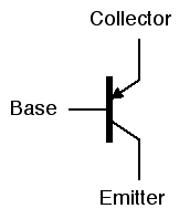
Transistors: A transistor is a solid-state electronic device with three
electrodes (a collector, a base, and an emitter) as shown on the right. It operates
like a switch between the collector and the emitter that is controlled by the base:
- if the base is given a high enough positive voltage then the switch is closed to allow
a current of positive charge to flow from the collector to the emitter - the transistor
is turned ON;
- if the base is given a very low voltage (close to 0) then the switch is opened to
block the flow of any current between the collector to the emitter - the transistor
is turned OFF.
|
 |
|
Note: The terms collector and emitter might be confusing. Each electron
has a negative charge so when a transistor is turned ON,
the electrons flow from the emitter to the collector.
Each transistor in a computer is a bi-stable device with each of its electrodes
(collector, base, or emitter) either:
- in the 1-state with a high positive voltage; or
- in the 0-state with a voltage close to zero.
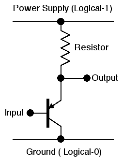
Every logic gate is powered by connecting it between:
- a power supply bus which is always in the 1-state with a high positive voltage; and
- a ground bus which is always in the 0-state with a zero voltage.
|
The Circuit for an AND-gate: The circuit for an AND-gate connects two transistors and a
resistor in series as shown on the right.
No current can flow through the transistors until the voltages of both Input-1 and Input-2 are raised
to the 1-state.
- If either input of the two transistors is in the 0-state then no current
flows through the transistors and the resistor pulls the output voltage down to the 0-state of the Ground bus.
- If both inputs to the transistors are in the 1-state then both transistors are turned ON and
their very low resistance pulls the output voltage up to the 1-state of the Power Supply bus
(the resistor limits the current flowing through the transistors to a safe value.)
Thus the state of the output of the circuit is the logical-AND of the states of the inputs
of the two transistors.
|  |
The Circuit for an OR-gate: The circuit for an OR-gate connects two parallel
transistors in series with a resistor as shown on the right.
- If both inputs of the two transistors are in the 0-state then both transistors
are turned OFF and the resistor pulls the output voltage down to the 0-state of the Ground bus.
- If the input to either transistor is in the 1-state then that transistor is
turned ON and its very low resistance pulls the output voltage up to the 1-state of the
Power Supply bus (the resistor limits the current flowing through the transistor to a safe value.)
Thus the state of the output of the circuit is the logical-OR of the states of the inputs
of the two transistors.
|  |
The Circuit for a NOT-gate: The circuit for a NOT-gate connects a resistor
and a single transistor in series as shown on the right.
- If the input to the transistor is in the 0-state then the transistor is turned OFF and
the resistor pulls the output voltage up to 1-state of the Power Supply bus.
- If the input to the transistor is in the 1-state then the transistor is turned ON and its
very low resistance pulls the output voltage down to the 0-state of the Ground bus
(the resistor limits the current flowing through the transistor to a safe value.)
Thus the state of the output of the circuit is the logical-NOT of the state of the input
to the transistor.
|  |
(4.4) Building Computer Circuits
A combinational circuit is a collection of logic gates:
- that transforms a set of binary inputs into a set of binary outputs; and
- where the values of the outputs depend only on the current values of the
inputs.
Figure 4.19 shows a combinational circuit, C, with m inputs and
n outputs.
A combinational circuit has no memory - every time one or more of its inputs
changes state (from 0 to 1 or from 1 to 0) the circuit forgets the old state of its
inputs and sets the values of its outputs based only on the new state of its inputs.
The behavior of a combinational circuit with m inputs can be described by a
truth table with 2m rows.
Example 1: As an example we develop the truth table of
the following combinational circuit that has two inputs, a and b,
and one output, z.
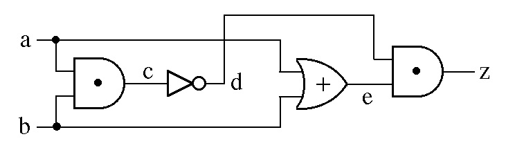 The circuit has two inputs, a and b, so the truth table has four rows:
The first two columns of the truth table, inputs a and b, show all
four possible combinations of the values of the inputs.
The state of internal line c = a AND b so column c
of the truth table equals 1 in only those rows where both columns a and
b equal 1.
The state of internal line d = NOT c so column d equals 1
where column c equals 0 and vice versa.
The state of internal line e = a OR b so column e
of the truth table equals 0 in only those rows where both
columns a and b equal 0.
The state of output z = d AND e so column z
of the truth table equals 1 in only those rows where both
columns d and e equal 1.
The circuit has two inputs, a and b, so the truth table has four rows:
The first two columns of the truth table, inputs a and b, show all
four possible combinations of the values of the inputs.
The state of internal line c = a AND b so column c
of the truth table equals 1 in only those rows where both columns a and
b equal 1.
The state of internal line d = NOT c so column d equals 1
where column c equals 0 and vice versa.
The state of internal line e = a OR b so column e
of the truth table equals 0 in only those rows where both
columns a and b equal 0.
The state of output z = d AND e so column z
of the truth table equals 1 in only those rows where both
columns d and e equal 1.
| Inputs | Internal Lines | Output |
|---|
| a | b | c | d | e | z |
|---|
0
0
1
1 |
0
1
0
1 |
0
0
0
1 |
1
1
1
0 |
0
1
1
1 |
0
1
1
0 |
|---|
We now remove the columns for the internal lines to obtain the truth table
of the circuit:
| Inputs | Output |
|---|
| a | b | z |
|---|
0
0
1
1 |
0
1
0
1 |
0
1
1
0 |
|---|
Notice that output z equals 1 if and only if inputs a and
b are in opposite states - one of the inputs must be a 1 and the other
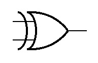
input must be a 0. A combinational circuit with this behavior is called an
exclusive-or circuit or an XOR circuit - it's used in many
places inside a computer and is usually shown with the following symbol:
Example 2:
As another example we develop the truth table for the following circuit that has
three inputs, a, b, and c, and two outputs, r and
s.
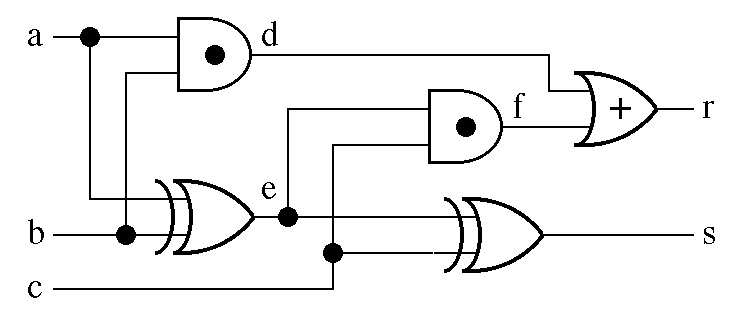 Since there are three inputs the truth table has 23 = 8 rows.
The input columns, a, b, and c, show all eight possible
combinations of the values of the inputs.
The state of internal line d = a AND b so column d
of the truth table equals 1 in only those rows where both columns a and
b equal 1.
The state of internal line e = a XOR b so column e
of the truth table equals 1 in only those rows where columns a and
b have opposite values.
The state of internal line f = c AND e so column f
of the truth table equals 1 in only those rows where both columns c and
e equal 1.
The state of output r = d OR f so column r
of the truth table equals 0 in only those rows where both
columns d and f equal 0.
The state of output s = c XOR e so column s
of the truth table equals 1 in only those rows where columns c and
e have opposite values.
Since there are three inputs the truth table has 23 = 8 rows.
The input columns, a, b, and c, show all eight possible
combinations of the values of the inputs.
The state of internal line d = a AND b so column d
of the truth table equals 1 in only those rows where both columns a and
b equal 1.
The state of internal line e = a XOR b so column e
of the truth table equals 1 in only those rows where columns a and
b have opposite values.
The state of internal line f = c AND e so column f
of the truth table equals 1 in only those rows where both columns c and
e equal 1.
The state of output r = d OR f so column r
of the truth table equals 0 in only those rows where both
columns d and f equal 0.
The state of output s = c XOR e so column s
of the truth table equals 1 in only those rows where columns c and
e have opposite values.
| Inputs | Internal Lines |
Outputs |
|---|
| a | b | c | d | e | f |
r | s |
|---|
0
0
0
0
1
1
1
1 |
0
0
1
1
0
0
1
1 |
0
1
0
1
0
1
0
1 |
0
0
0
0
0
0
1
1 |
0
0
1
1
1
1
0
0 |
0
0
0
1
0
1
0
0 |
0
0
0
1
0
1
1
1 |
0
1
1
0
1
0
0
1 |
We now remove the internal-line columns of this table to obtain the truth table
for the circuit.
| Inputs | Outputs |
|---|
| a | b | c | r | s |
|---|
0
0
0
0
1
1
1
1 |
0
0
1
1
0
0
1
1 |
0
1
0
1
0
1
0
1 |
0
0
0
1
0
1
1
1 |
0
1
1
0
1
0
0
1 |
To see what this circuit does let's swap the two rows in the middle of the truth
table and then group together those rows with identical outputs:
| Inputs | Outputs |
|---|
| a | b | c | r | s |
|---|
| 0 | 0 | 0 | 0 | 0 |
|---|
0
0
1 |
0
1
0 |
1
0
0 |
0
0
0 |
1
1
1 |
0
1
1 |
1
0
1 |
1
1
0 |
1
1
1 |
0
0
0 |
| 1 | 1 | 1 | 1 | 1 |
|---|
What's the common characteristic of the three input columns in each group of rows?
The truth table of a combinational circuit with n inputs and one output has
2n rows so any algorithm to construct the truth table has at least a
θ(2n) running time. In section 3.5 we saw that
algorithms with θ(2n) running times can only be used
for small values of n.
(4.4.2) A Circuit Construction Algorithm:
Examples 1 and 2 above illustrate how one
can analyze a given combinational circuit to obtain its truth table and
see how it behaves. In this section we examine the reverse process;
i.e., how one can synthesize (construct) any combinational circuit from
its truth table.
Product Circuits: A combinational circuit with a single output where
the output column of the truth table contains just a single 1 is called a product
circuit since it can be constructed using just AND-gates and NOT-gates. For
example, suppose the truth table is:
| Inputs | Output |
|---|
| a | b | c | z |
|---|
0
0
0
0
1
1
1
1 |
0
0
1
1
0
0
1
1 |
0
1
0
1
0
1
0
1 |
0
0
1
0
0
0
0
0 |
The output of this circuit, z, should equal 1 if and only if
a = 0, b = 1, and c = 0, so:
z = (NOT(a ) AND b ) AND (NOT(c )).
One can use two NOT-gates and two AND-gates to construct this product circuit:

Single-Output Circuits: Suppose the truth table has only one output column.
If the column contains only a single 1 then it is a product circuit that can be
constructed as described in the previous item.
If the output column contains multiple 1's then the circuit can be constructed
as a Sum-of-Products - a product circuit is constructed for each 1
in the output column and then the outputs of these product circuits are combined
with a set of OR-gates. To illustrate the construction we consider just the
s output of the Example 2 circuit described above.
The truth table of this single-output circuit is:
| Inputs | Output |
|---|
| a | b | c | s |
|---|
0
0
0
0
1
1
1
1 |
0
0
1
1
0
0
1
1 |
0
1
0
1
0
1
0
1 |
0
1
1
0
1
0
0
1 |
The output column contains four 1's so a product circuit is
constructed for each of the 1's and then the outputs of these four product
circuits are combined with three OR-gates as shown in the following diagram:
 The sum-of-products construction always produces a circuit but not necessarily
the optimal circuit. For example, if we examine the circuit diagram of
Example 2 above we see that the s output of the circuit
only requires its two XOR-circuits. The circuit diagram of
Example 1 above shows that each XOR-circuit can be constructed
from 2 AND-gates, 1 OR-gate, and 1 NOT-gate. The following table compares the
gate-counts of the Sum-of-Products construction described here with the
construction using two XOR-circuits.
The sum-of-products construction always produces a circuit but not necessarily
the optimal circuit. For example, if we examine the circuit diagram of
Example 2 above we see that the s output of the circuit
only requires its two XOR-circuits. The circuit diagram of
Example 1 above shows that each XOR-circuit can be constructed
from 2 AND-gates, 1 OR-gate, and 1 NOT-gate. The following table compares the
gate-counts of the Sum-of-Products construction described here with the
construction using two XOR-circuits.
| Construction | AND-gates | OR-gates |
NOT-gates |
|---|
| Sum-of-Products | 8 | 3 | 3 |
|---|
| Two XOR-circuits | 4 | 2 | 2 |
|---|
Problem: How many OR-gates are required to sum up the outputs of N
product circuits? Does the arrangement of the OR-gates make any
difference?
Multiple-Output Circuits: If the truth table has more than one output
column then one simply builds a single-output circuit for each of the output
columns. This is the Sum-of-Products Construction Algorithm shown in Figure
4.23 of the text - it produces a combinational circuit for any truth table
but it doesn't always produce the optimal circuit with the minimum gate count.
Any combinational circuit produced by the algorithm uses just AND-gates, OR-gates,
and NOT-gates - we need no other kinds of building blocks beyond those shown in
Figure 4.10 of the text.
(4.4.3) Examples of Circuit Design and Construction: Here we design a
compare-for-equality circuit and an addition circuit.
- Compare-for-Equality Circuit: The single output of this circuit
equals 1 if and only if two N-bit unsigned binary numbers,
aN-1aN-2...a0 and
bN-1bN-2...b0, have equal values.
The two numbers have equal values if and only if their bits have the same value
in all N bit positions: ai = bi for all i = 0, 1, ..., N-1.
The text designs a circuit, 1-CE, for comparing two one-bit
numbers (Figure 4.22) and then uses it as a building block to construct a circuit
to compare N-bit numbers (Figure 4.23).
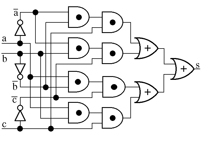
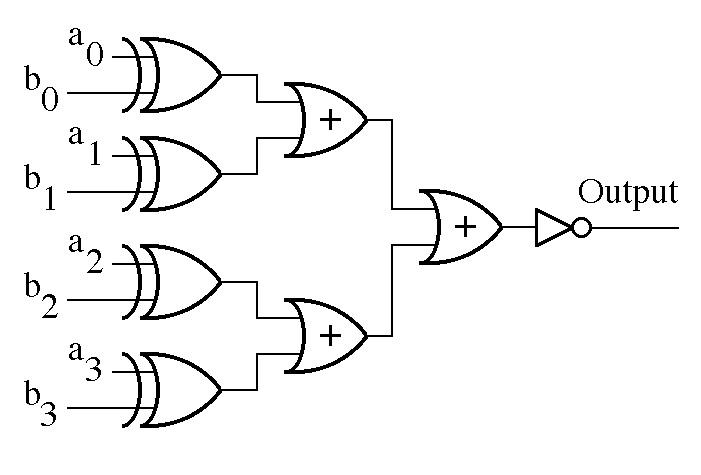
A different construction is possible: build a Compare-for-Inequality circuit and then
negate its output with a NOT-gate. N XOR circuits are used to
detect if any pair of corresponding bits, ai and bi, disagree in
any bit position, i = 0, 1, ..., N-1; the outputs of the XOR circuits are summed
together with a set of OR-gates; and a NOT-gate negates the output of the sum. The
following diagram shows a circuit for N = 4.
- Addition Circuit: The addition circuit adds two unsigned
N-bit binary integers, a and b, together to create an
(N+1)-bit binary sum, s. The bits of these numbers are given
subscripts as follows:
| aN-1 |
aN-2 | . . . |
a1 | a0 |
|---|
| + | bN-1 |
bN-2 | . . . |
b1 | b0 |
|---|
| ______________________________ |
|---|
| sN | sN-1 |
sN-2 | . . . |
s1 | s0 |
|---|
An algorithm for addition of two binary numbers is similar to the algorithm in
Figure 1.2 for the addition of two decimal numbers:
| Step 1: | Set the value of c0 to 0.
|
| Step 2: | Set | the value of i
equal to the value 0. |
| Step 3: | Repeat the instructions in steps 4
through 6 until the value of i is greater than N-1. |
| Step 4: | |
Add the two digits ai and bi to the current value of
ci to get si. |
| Step 5: | |
If si > 1, then reset si to (si - 2) and set
the value of ci+1 to 1; otherwise, set the value of
ci+1 to 0.
|
| Step 6: | |
Add 1 to i, effectively moving one column to the left. |
| Step 7: |
Set sN to the value of cN
|
| Step 8: |
Print out the final answer, sNsN-1sN-2...s0.
|
| Step 9: | Stop. |
First we construct a circuit, 1-ADD, to handle one of the bit places (this
circuit is usually called a full adder.)
The inputs to bit place i are bit ai, bit
bi, and a carry bit, ci,
from bit place (i -1) on the right. The outputs of bit place i
are bit si of the sum, s, and a carry bit,
ci+1, which is sent to bit place (i +1) on the left.
The truth table for bit place i is:
| INPUTS | Sum of
inputs |
OUTPUTS |
|---|
| ai | bi |
ci | ci+1 |
si |
|---|
| 0 | 0 | 0 | 0 | 0 | 0 |
|---|
| 0 | 0 | 1 | 1 | 0 | 1 |
|---|
| 0 | 1 | 0 | 1 | 0 | 1 |
|---|
| 0 | 1 | 1 | 2 | 1 | 0 |
|---|
| 1 | 0 | 0 | 1 | 0 | 1 |
|---|
| 1 | 0 | 1 | 2 | 1 | 0 |
|---|
| 1 | 1 | 0 | 2 | 1 | 0 |
|---|
| 1 | 1 | 1 | 3 | 1 | 1 |
|---|
Figure 4.26 in the text shows a Sum-of-Products construction of the 1-ADD
circuit but the Example 2 circuit has the same truth
table (after the column labels are changed) and is much simpler so it's a
better way of building the 1-ADD circuit. Figure 4.27 shows how
N of these circuits are connected together to build a circuit that
will add two N-bit binary numbers together:
This adder circuit is called a Carry Ripple Adder because
it doesn't complete the addition until all carries have rippled through a
chain of 1-ADD circuits. The worst case occurs when c1
must ripple through all (N-2) intervening stages to reach bit place
N-1. For large N the time spent in rippling carries slows the
adder down appreciably - a Carry Lookahead Adder is much faster.
(4.5) Control Circuits
Decoders: An N-to-2N decoder has N input
lines numbered N-1, N-2, ..., 1, 0, and 2N output
lines numbered 0, 1, ..., 2N-1. The decoder interprets the input
lines as bits of a binary number and sets the corresponding output line to a 1:
all other output lines are set to 0. For example, the truth table of a 3-to-8
decoder is:
| INPUTS | OUTPUTS |
|---|
| 2 | 1 | 0 | 0 | 1 | 2 | 3 |
4 | 5 | 6 | 7 |
| 0 | 0 | 0 |
1 | 0 | 0 | 0 |
0 | 0 | 0 | 0 |
|---|
| 0 | 0 | 1 |
0 | 1 | 0 | 0 |
0 | 0 | 0 | 0 |
|---|
| 0 | 1 | 0 |
0 | 0 | 1 | 0 |
0 | 0 | 0 | 0 |
|---|
| 0 | 1 | 1 |
0 | 0 | 0 | 1 |
0 | 0 | 0 | 0 |
|---|
| 1 | 0 | 0 |
0 | 0 | 0 | 0 |
1 | 0 | 0 | 0 |
|---|
| 1 | 0 | 1 |
0 | 0 | 0 | 0 |
0 | 1 | 0 | 0 |
|---|
| 1 | 1 | 0 |
0 | 0 | 0 | 0 |
0 | 0 | 1 | 0 |
|---|
| 1 | 1 | 1 |
0 | 0 | 0 | 0 |
0 | 0 | 0 | 1 |
|---|
Each output column of the truth table for an N-to-2N decoder
contains a single 1 so one can build the decoder with 2N product
circuits but that requires (N - 1) * 2N AND-gates plus N
NOT-gates. There's another construction technique for decoder circuits that requires
far less AND-gates. A 1-to-2 decoder requires only one NOT-gate:
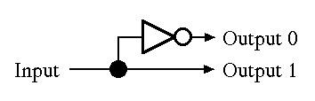 Figure 4.24 in the text shows a 2-to-4 decoder circuit but we redraw the circuit
to show that it requires four AND-gates plus two 1-to-2 decoders:
Figure 4.24 in the text shows a 2-to-4 decoder circuit but we redraw the circuit
to show that it requires four AND-gates plus two 1-to-2 decoders:
 A 4-to-16 decoder requires 16 AND-gates (arranged in a 4-by-4 array) plus two
2-to-4 decoders:
A 4-to-16 decoder requires 16 AND-gates (arranged in a 4-by-4 array) plus two
2-to-4 decoders:
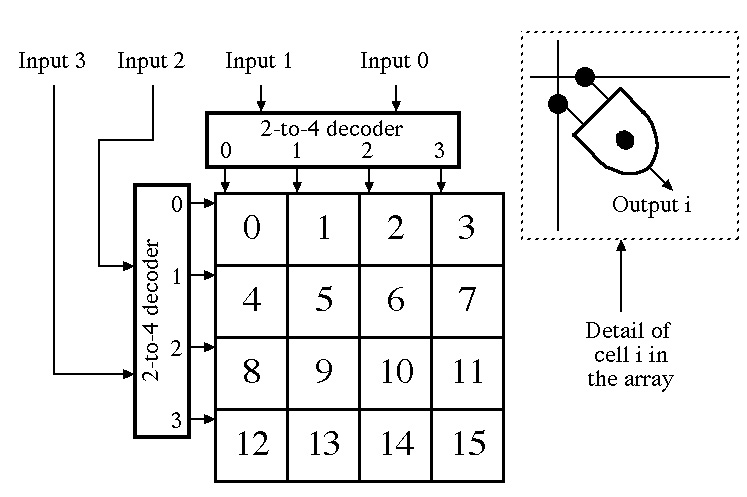 One 2-to-4 decoder selects one row of the 4-by-4 array by sending a 1-value on one
of the horizontal lines of the array depending on the values of Input 3 and
Input 2.
The other 2-to-4 decoder selects one column of the array by sending a 1-value on
one of the vertical lines of the array depending on the values of Input 1
and Input 0.
Only the AND-gate in the selected row of the selected column sees
1-values on both of its inputs so it's the only AND-gate in the array that sets
its output to 1.
One 2-to-4 decoder selects one row of the 4-by-4 array by sending a 1-value on one
of the horizontal lines of the array depending on the values of Input 3 and
Input 2.
The other 2-to-4 decoder selects one column of the array by sending a 1-value on
one of the vertical lines of the array depending on the values of Input 1
and Input 0.
Only the AND-gate in the selected row of the selected column sees
1-values on both of its inputs so it's the only AND-gate in the array that sets
its output to 1.
Very large decoders are constructed with this technique. For example, a 64-megabit
RAM chip holds 226 = 67,108,864 memory bits and uses a
26-to-226 decoder circuit to select one of its memory bits to be read
or written. The decoder circuit requires 226 AND-gates (arranged in a
8192-by-8192 array) plus two 13-to-8192 decoder circuits. Each 13-to-8192
decoder circuit requires 8192 AND-gates (arranged in a 64-by-128 array) plus one
6-to-64 decoder circuit plus another 7-to-128 decoder circuit - these decoder
circuits use smaller decoder circuits, etc., etc.
Multiplexors: A multiplexor is used to select data from one of a number
of sources to send to a particular destination - for example, it might be used to
select data from one of a number of registers to send to an adder circuit.
A 2N-input multiplexor is a switch with 2N input lines,
one output, and N selector lines: the states of the selector
lines determine which input line sends its value to the output. Figure 4.28 shows the
design of a 2-input multiplexor.
Its truth table is:
| Selector line | Input line 0 | Input line 1 |
Output |
|---|
| 0 | 0 | 0 | 0 |
|---|
| 0 | 0 | 1 | 0 |
|---|
| 0 | 1 | 0 | 1 |
|---|
| 0 | 1 | 1 | 1 |
|---|
| 1 | 0 | 0 | 0 |
|---|
| 1 | 0 | 1 | 1 |
|---|
| 1 | 1 | 0 | 0 |
|---|
| 1 | 1 | 1 | 1 |
|---|
When the Selector line state is 0 the state of Input line 0 is sent to the Output -
when the Selector line state is 1 the state of Input line 1 is sent to the Output.
A 2N-input multiplexor can be constructed using an
N-to-2N decoder plus 2N AND-gates plus (2N - 1)
OR-gates. The following diagram shows the circuit of a 4-input multiplexor - the
decoder outputs allow one of the AND-gates to send the state of its Input line into
the set of OR-gates (all other AND-gates send in 0's) and the set of OR-gates route
that Input line state to the output of the multiplexor:

Kenneth E. Batcher - 12/30/2007